Yeasu FT301D Restore - Part 1
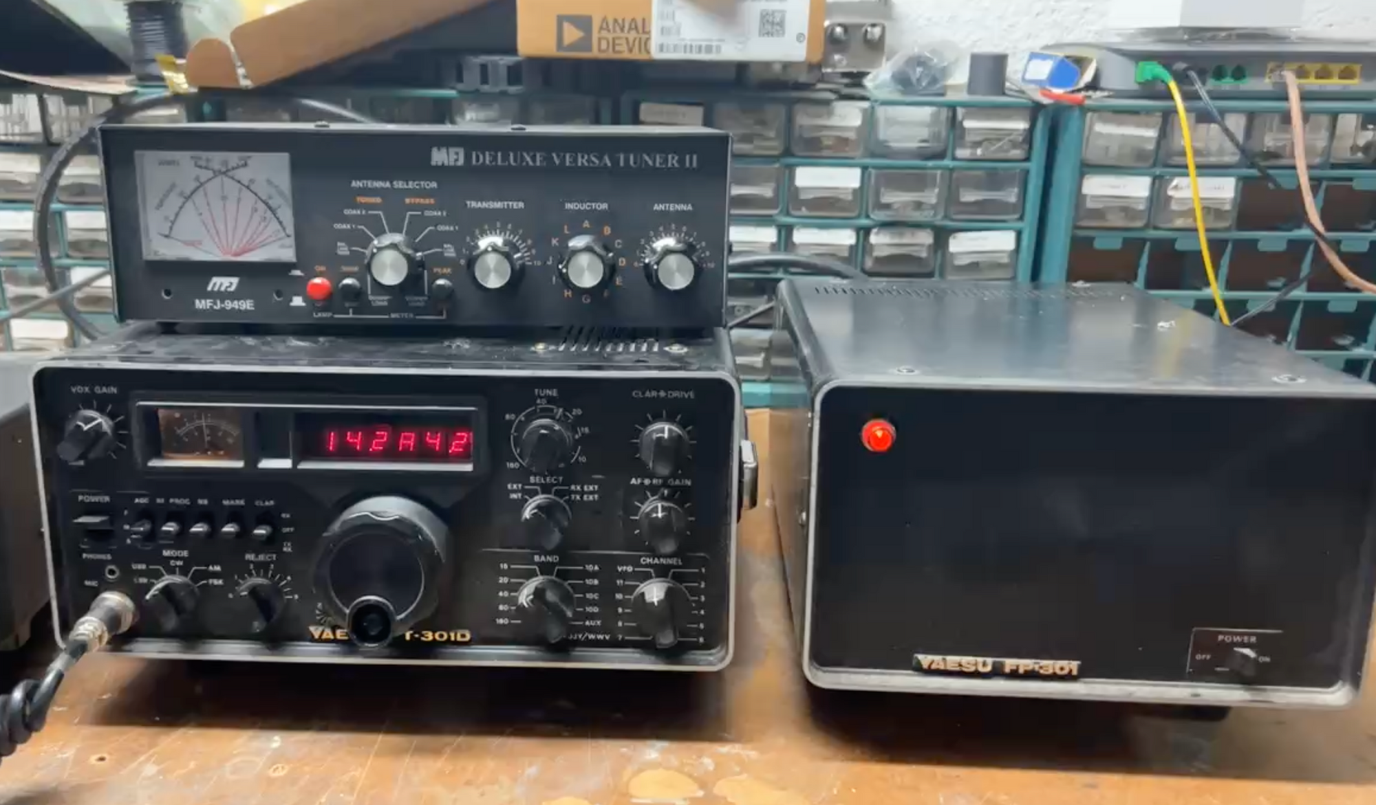
When I first got my ham radio license I purchased a Yaesu FT-301D from another amatuer radio operator on Craiglist. I enjoyed using the radio, but over the years I've ended up using other radios that were either more reliable or matched my requirements better (QRP, portable, etc). At this point the radio has been sitting around for 10+ years and is in need of alignment and some repair. I'm going to document that process in a series of logs.

I really like operating and working on this radio. Its easy to work on and well constructed. Many of the modules are implemented on card slots that are removeable and make it easy to gain access for debug.

I purchased a riser/extension card on eBay that lets me get access to the cards for debug. This is very helpful – without it I was having to solder on wires in order to probe at the cards during operation.

The user manual has a full schematic and block diagram. There is also a functional description of each circuit and a complete electrical BOM. The alignment procedures are included at the end.
My plan is to work through the alignment procedure outlined in the manual and stop every time I notice an issue. I don't expect too many problems because the radio is generally working okay and was working fine at one point.
The setup for the first step of alignment involves transmitting on CW. I attached a dummy load to the radio and keyed up to find almost no output. There were no issues on AM, LSB and USB modes, but the output fell to zero for CW. Below is the section of the block diagram showing the path that the CW carrier takes through the radio. The output of an oscillator located on the IF UNIT board is amplified, passed over to the FILTER UNIT to be filtered by a crystal bandpass filter (XF92A) and then to the NB UNIT for amplification:

I checked the output of the IF UNIT and found a weak 9 MHz signal at the output of the filter board. The amplitude was about 5 mVrms. It seemed likely the oscillator was working fine because the signal was the correct frequency. I checked the schematic for the IF Unit in the manual:

The two transistors related to the CW carrier are located in the upper right. I found a small error in the schematic included in the manual. As shown, the Q403 transistor will not be properly powered. I used the PCB to re-draw that portion of the schematic:

Do you see the difference? (Hint: R415 is routed differently).
Using the correct schematic I checked the bias of each of the transistors and the DC operating point of a few points in the circuit. Everything looked normal. I traced the CW signal from the oscillator to the output using an oscilloscope. All the levels looked reasonable.
Next I checked the FILTER UNIT. I found no signal at the output of the FILTER_UNIT. I traced across the board and found that the signal was being filtered by the SSB Filter crystal filter (XF92A). This crystal is centered at 9000.000 kHz. I checked the frequency of the CW carrier and found it was a bit low at 8998.0 kHz vs. the target frequency of 8999.300 kHz. I adjusted TC401 variable capacitor on the IF unit to adjust the clock frequency, but the overall range of adjustment was too low.

I removed the fixed capacitor, C428, from the IF UNIT board and that brought the frequency up into a range where I could tune it to 8999.3 kHz.

After adjusting the CW carrier frequency I was able to measure 5 mVrms at the output SSB filter and further confirmed that the radio was now generating >100W at the dummy load. Problem solved!
Done for now.